Products & Technologies

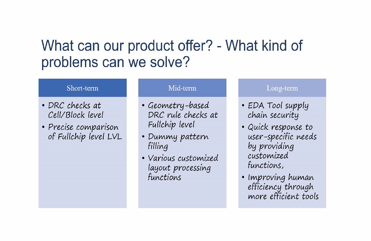
Our orientation is products and technologies and our goal is fulfilling real needs from our customers. Our tools  innovates continuously bottom algorithm to build a key EDA tool chain

High-efficiency process of large layout files and large amount of patterns

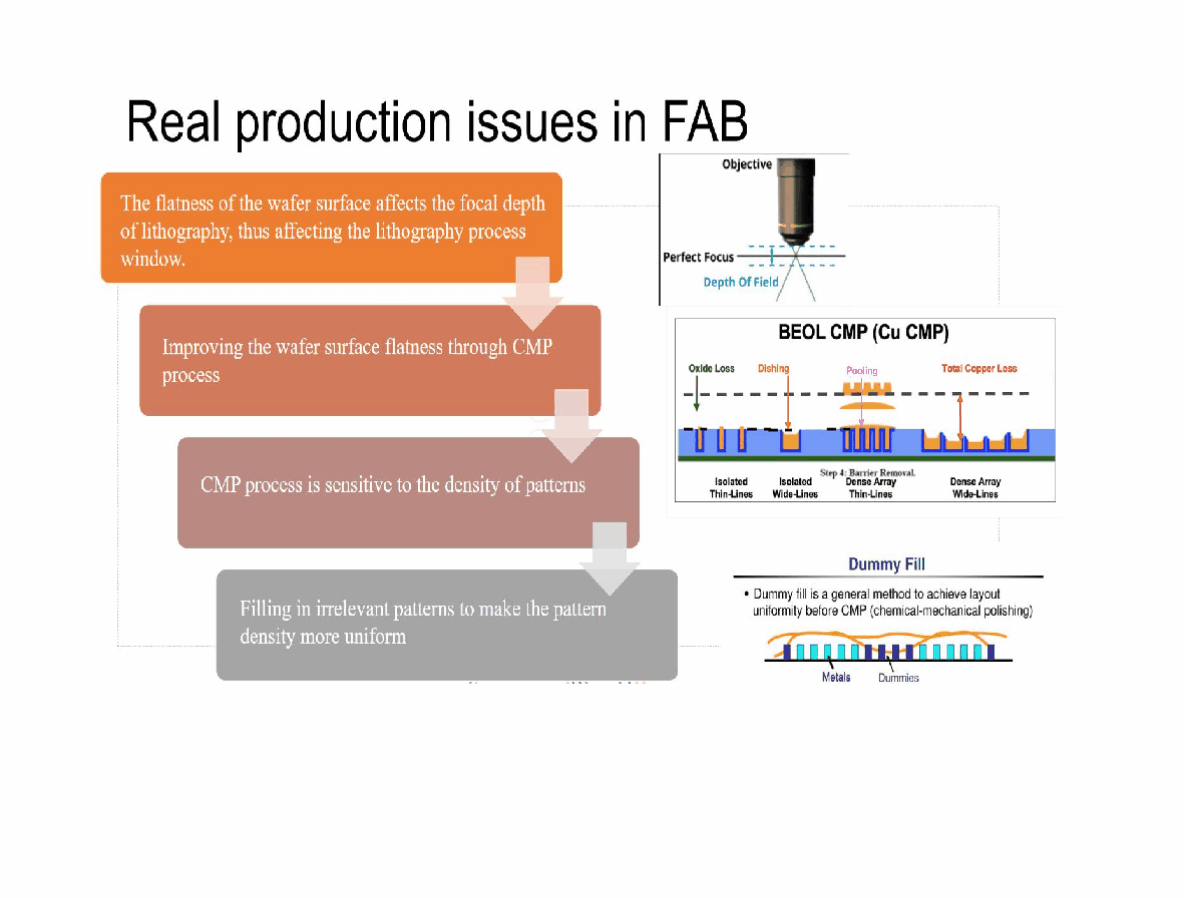
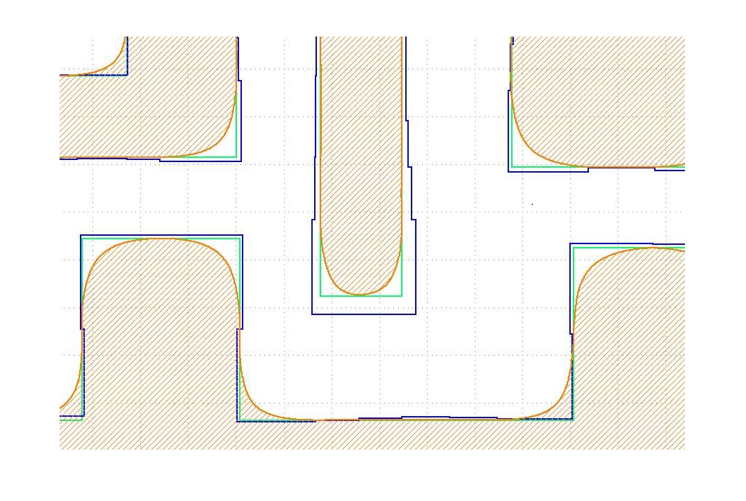
Using fast and accurate physical and mathematical model to obtain simulation results which are more matching to reality to assist advanced tech node RD and yield enhancement.

Physical Verification Platform
Use sofcheck pattern and connectivity for standard unit and connecting pattern based on layout hierarchy
Provide fast and accurate design rule check, shorten chip design period, accelerate market entry of chips
Use deep learning to extract design rules, build design rule base depended on pattern
Reduce workload of manual coding of design rules, improve automation of design rule extraction and pattern detection
Chip Layout Dummy Fill Product
By inserting dummy patterns in the production layout, it can effectively improve the wafer surface flatness of the CMP process and enlarge the process window
Supports the addition of various dummy patterns, real-time density checks, andcorrection, etc.
Supports basic DRC commands for post-fill layout inspection, such as distance measurement, density check, etc
Litho Modeling
Use computer to simulate lithography process of chip manufacture to obtain image of mask on wafer. Through comparing wafer image and target pattern, expose the uncertainty of lithography before manufacturing as soon as possible and use technical methods to improve image quality
Provide fast and accurate simulation model and apply the model in different usage scenes to help customers solve practical problems
Yixin Technology is always ready to help chip manufacturers!
Please complete this form to receive more information, including product trials, quotes and demos.